Emergent Network of Narrow Transport Channels

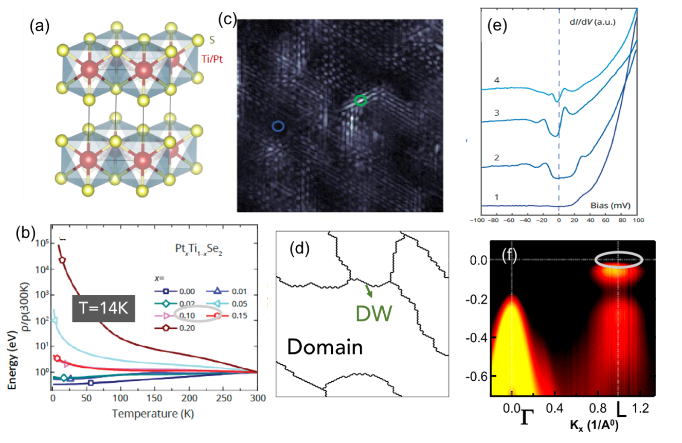
A new route for a metal to insulator transition, driven by the creation of a network of narrow channels, has been discovered. When Pt is substituted for Ti in 1T-TiSe2 (panel (a)), a self-doped charge-density wave material, the resistivity shows a dramatic increase by five orders of magnitude (panel (b)). Akin to a stone creating cracks in an ice-sheet, the impact of Pt creates domain walls (panel (c),(d)) of nanometer size diameter that suck charge from the bulk leaving a hard insulating gap in the bulk (panel (e), scan (1)). The charges now confined to narrow channels interact strongly forming a pseudogap, similar to a Luttinger liquid, as seen in the local density of states by scanning tunneling spectroscopy (STM) (panel (e), scan (3,4)), and further corroborated by angle resolved photoemission spectroscopy (ARPES) that shows a pseudogap opening up at the L-point at low temperatures.
