
Emergent Network of Narrow Transport Channels

Jan 22, 2021
(a) Crystal structure of 1T-TiSe2 with Pt substituting for Ti; (b) temperature-dependent transport, STM showing topography (c) and spectroscopy (e), (d) schematic of domain walls, ARPES showing pseudogap formation at the L point.

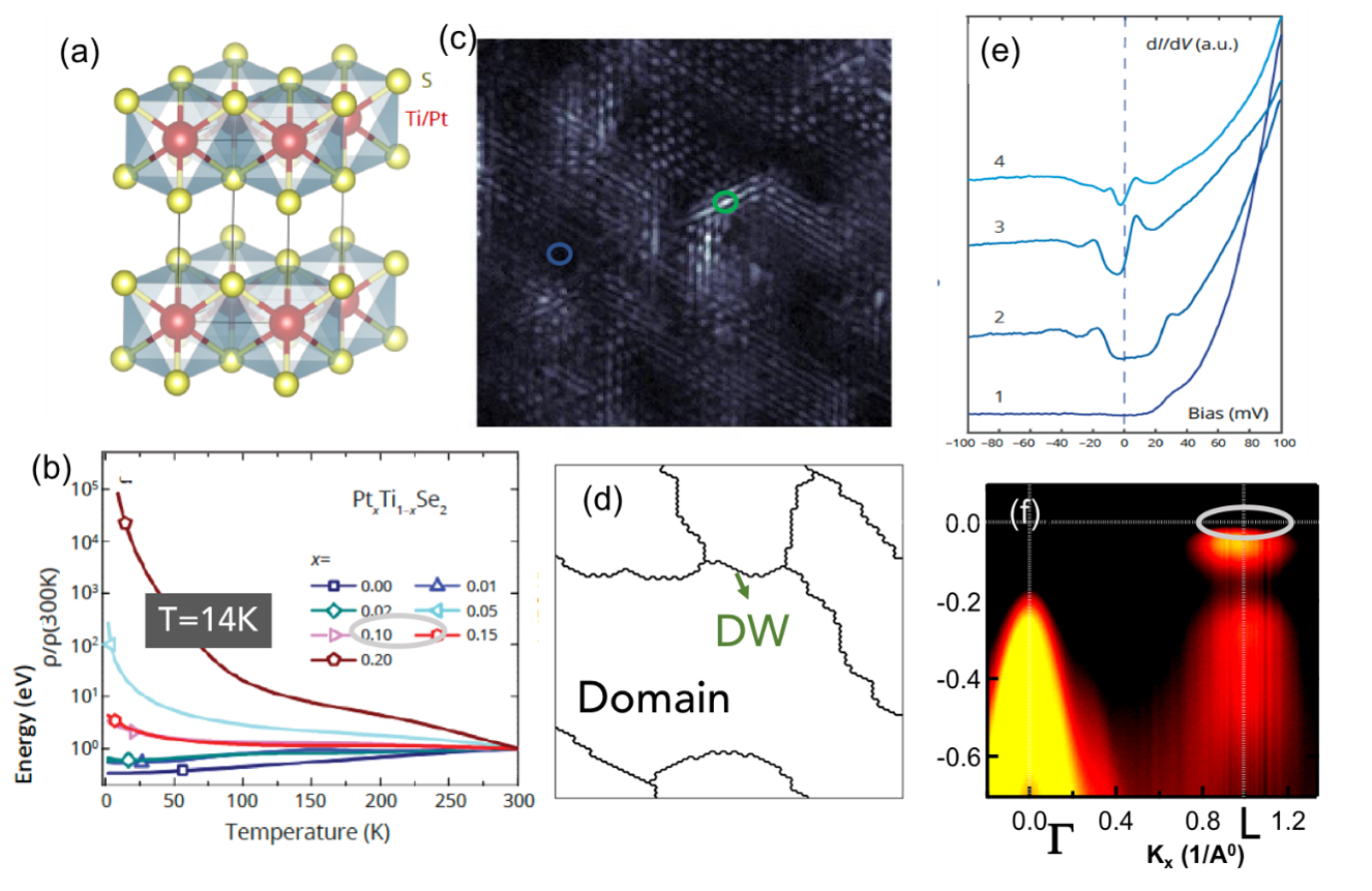
A new route for a metal to insulator transition, driven by the creation of a network of narrow channels, has been discovered. When Pt is substituted for Ti in 1T-TiSe2 (panel (a)), a self-doped charge-density wave material, the resistivity shows a dramatic increase by five orders of magnitude (panel (b)). Akin to a stone creating cracks in an ice-sheet, the impact of Pt creates domain walls (panel (c),(d)) of nanometer size diameter that suck charge from the bulk leaving a hard insulating gap in the bulk (panel (e), scan (1)). The charges now confined to narrow channels interact strongly forming a pseudogap, similar to a Luttinger liquid, as seen in the local density of states by scanning tunneling spectroscopy (STM) (panel (e), scan (3,4)), and further corroborated by angle resolved photoemission spectroscopy (ARPES) that shows a pseudogap opening up at the L-point at low temperatures.

Authors

N. Trivedi (OH St. U.), V. Madhavan (UIUC), U. Chatterjee (U. VA), E. Morosan (Rice U.)

Additional Materials

U.S. National Science Foundation and NSF DMREF, Materials for Our Future

This material is based upon work supported by the U.S. National Science Foundation Award No. 2015237. Any opinions, findings, and conclusions or recommendations expressed in this material are those of the author(s) and do not necessarily reflect the views of the U.S. National Science Foundation. This site is maintained collaboratively by principal investigators with NSF DMREF awards, independent of the NSF.