Tunable Semiconductors: Organic-inorganic Hybrids
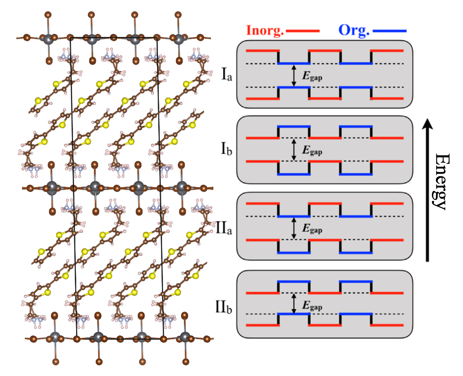
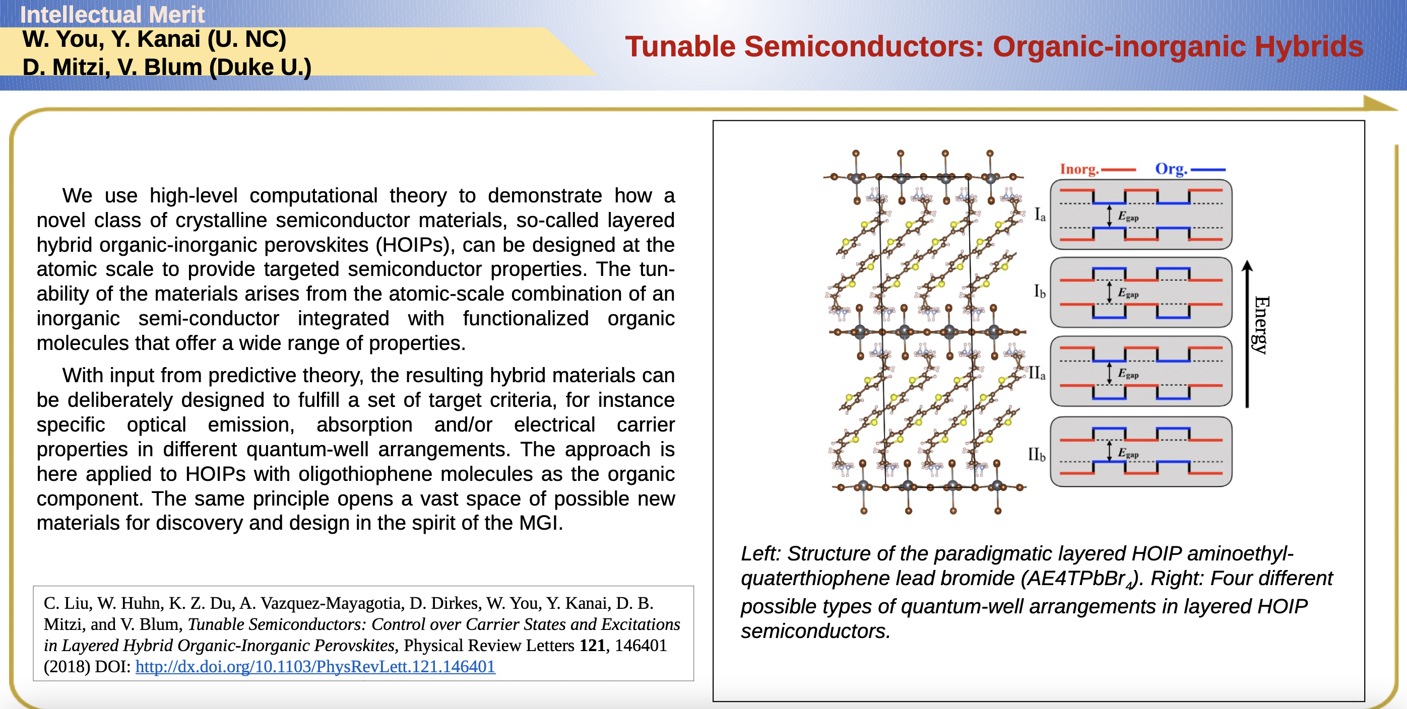
We use high-level computational theory to demonstrate how a novel class of crystalline semiconductor materials, so-called layered hybrid organic-inorganic perovskites (HOIPs), can be designed at the atomic scale to provide targeted semiconductor properties. The tun-ability of the materials arises from the atomic-scale combination of an inorganic semi-conductor integrated with functionalized organic molecules that offer a wide range of properties.
With input from predictive theory, the resulting hybrid materials can be deliberately designed to fulfill a set of target criteria, for instance specific optical emission, absorption and/or electrical carrier properties in different quantum-well arrangements. The approach is here applied to HOIPs with oligothiophene molecules as the organic component. The same principle opens a vast space of possible new materials for discovery and design in the spirit of the MGI.