Designing Contact Independent High-performance Low-Cost Flexible Electronics
Simulations were used to identify the fabrication window wherein the Organic Field Effect Transistor (OFET) mobility is decoupled from the work function of the contact. This knowledge was then exploited to guide the design of low-cost, high-mobility devices on flexible substrates for which all layers are solution-deposited.
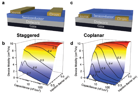
By using simulations to guide design, it was possible to virtually explore over 2000 different device configurations. This efficient approach significantly reduced the need for physical prototypes, requiring only a few experimental devices to validate predictions and confirm the hypothesis. The success highlights the value of this design process, which considers a wide range of device parameters and identifies optimal configurations that achieve high mobility irrespective of the Schottky barrier height at the electrode/organic semiconductor interface.
By pinpointing the critical elements of barrier-tolerant OFET architectures, it was possible to successfully adapt the fabrication process to create all-solution-processed transistors on flexible substrates. These devices yield mobilities exceeding 5 cm2 V−1 s−1, which is the highest obtained so far in all-solution-processed OFETs.
