Designing Materials for Next-generation Spintronic Devices

Our team works in a closed-loop fashion to integrate p-bit theory, high-throughput materials screening, first-principles calculations, wafer-scale combinatorial material synthesis, fast turnaround material and device characterizations, and atom-to-system modular simulations, to accelerate materials discovery and lay the foundation for a probabilistic computer.
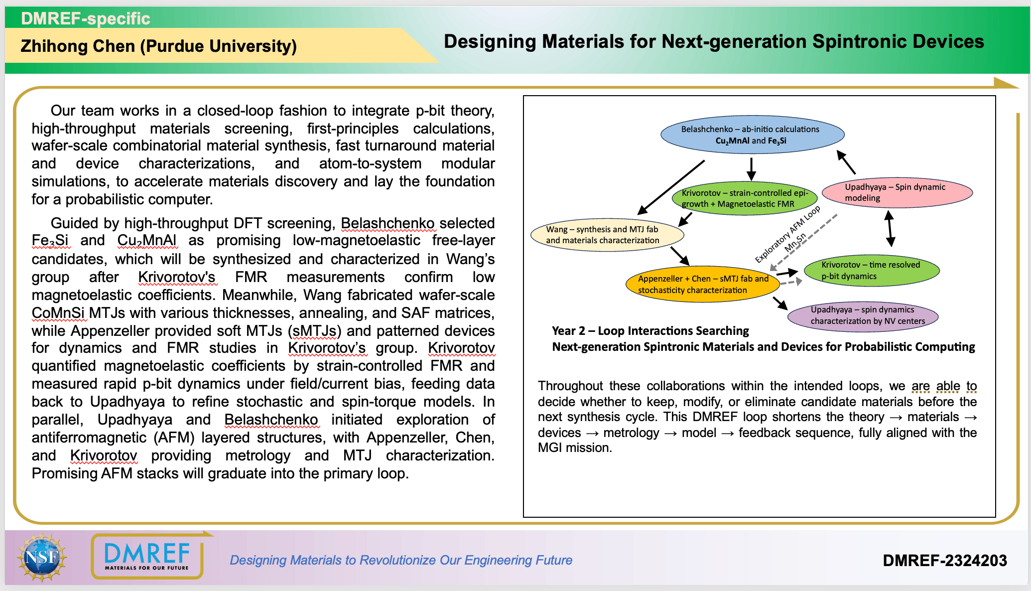
Guided by high-throughput DFT screening, Belashchenko selected Fe₃Si and Cu₂MnAl as promising low-magnetoelastic free-layer candidates, which will be synthesized and characterized in Wang’s group after Krivorotov's FMR measurements confirm low magnetoelastic coefficients. Meanwhile, Wang fabricated wafer-scale CoMnSi MTJs with various thicknesses, annealing, and SAF matrices, while Appenzeller provided soft MTJs (sMTJs) and patterned devices for dynamics and FMR studies in Krivorotov’s group. Krivorotov quantified magnetoelastic coefficients by strain-controlled FMR and measured rapid p-bit dynamics under field/current bias, feeding data back to Upadhyaya to refine stochastic and spin-torque models. In parallel, Upadhyaya and Belashchenko initiated exploration of antiferromagnetic (AFM) layered structures, with Appenzeller, Chen, and Krivorotov providing metrology and MTJ characterization. Promising AFM stacks will graduate into the primary loop.