Strain at Interfaces in Organic Devices
Jul 1, 2017
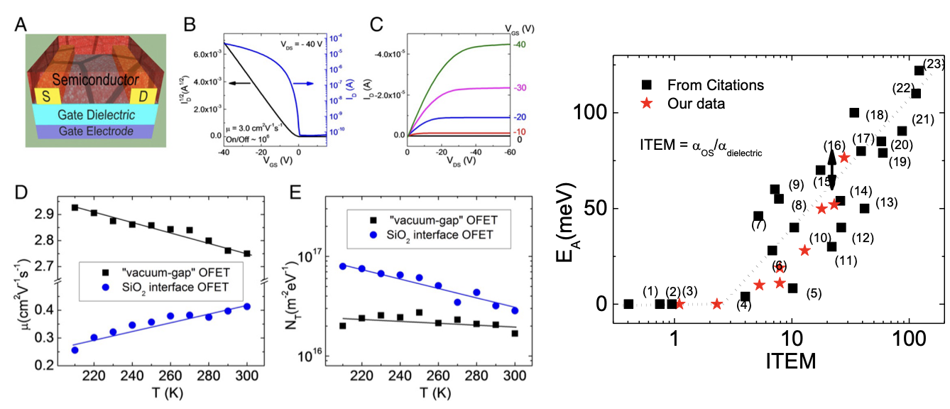
- The impact of inhomogeneous strain induced in an organic semiconductor was evaluated by virtue of the mismatch in the coefficients of thermal expansion of the consecutive layers on the transistor properties.
- Through a combined theoretical and experimental approach, it was found that thermal strain increases the interfacial electronic trap density, lowers the effective mobility, and can induce a crossover from band-like to activated transport irrespective of the device design.
- The existence of a universal scaling between the activation energies of charge transport and the relative mismatch of the thermal expansion of the semiconductor and dielectric layers was confirmed.
- These results provide evidence that a high-quality organic semiconductor layer is not sufficient to obtain efficient charge-carrier transport and underline the importance of evaluating a broad range of material properties where they are brought in contact.