A Simple and Robust Approach to Reducing Contact Resistance in Organic Transistors
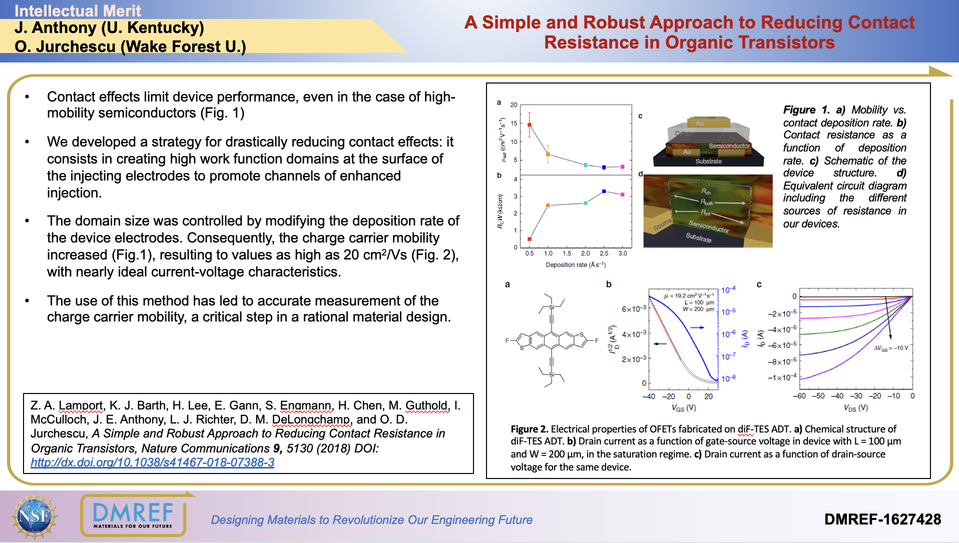
Contact effects limit device performance, even in the case of high-mobility semiconductors (Fig. 1)
We developed a strategy for drastically reducing contact effects: it consists in creating high work function domains at the surface of the injecting electrodes to promote channels of enhanced injection.
The domain size was controlled by modifying the deposition rate of the device electrodes. Consequently, the charge carrier mobility increased (Fig.1), resulting to values as high as 20 cm2/Vs (Fig.2), with nearly ideal current-voltage characteristics.
The use of this method has led to accurate measurement of the charge carrier mobility, a critical step in a rational material design.
Figure 1. a) Mobility vs. contact deposition rate. b) Contact resistance as a function of deposition rate. c) Schematic of the device structure. d) Equivalent circuit diagram including the different sources of resistance in our devices.
Figure 2. Electrical properties of OFETs fabricated on diF-TES ADT. a) Chemical structure of diF-TES ADT. b) Drain current as a function of gate-source voltage in device with L = 100 µm and W = 200 µm, in the saturation regime. c) Drain current as a function of drain-source voltage for the same device.