Research Highlights
Discovery of Tunable Quantum Anomalous Hall Octet
2/16/2023 | Fan Zhang (University of Texas at Dallas)
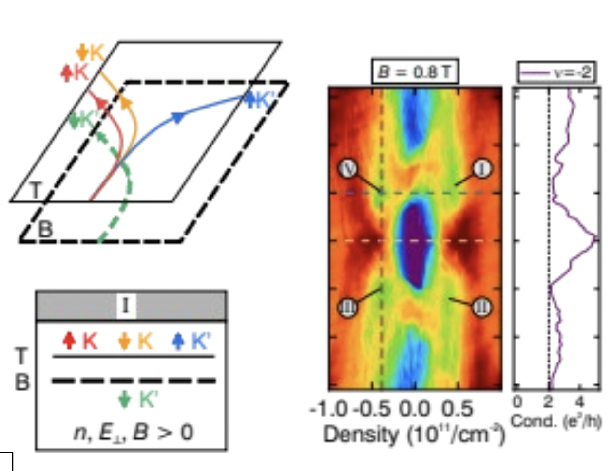
Bernal bilayer graphene is a naturally occurring system with neither spin-orbit coupling nor moiré complex. •Quantum anomalous Hall (QAH) octet, i.e., eight states exhibiting quantum Hall effect at zero magnetic field, was theoretically predicted and experimentally observed.
Self-assembled Block Polymers with Complete Photonic Band Gaps
2/10/2023 | Glenn H. Fredrickson and Kevin D. Dorfman
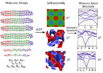
We have developed a workflow that allows for theoretical prediction of photonic crystals formed from bottom-up self assembly of block polymers. Using established self-consistent field theory (SCFT) methods, we are able to predict the symmetries of stable periodic structures formed at lengths scales of 10s-100s nm by such materials. Following structure prediction, photonic band structures are predicted by solving Maxwell’s equations on the resulting periodic dielectric profile.
Controlling Supramolecular Chirality in Peptide-p-peptide Networks
2/8/2023 | J. Tovar (Johns Hopkins U.) A. Ferguson (U. Chicago)
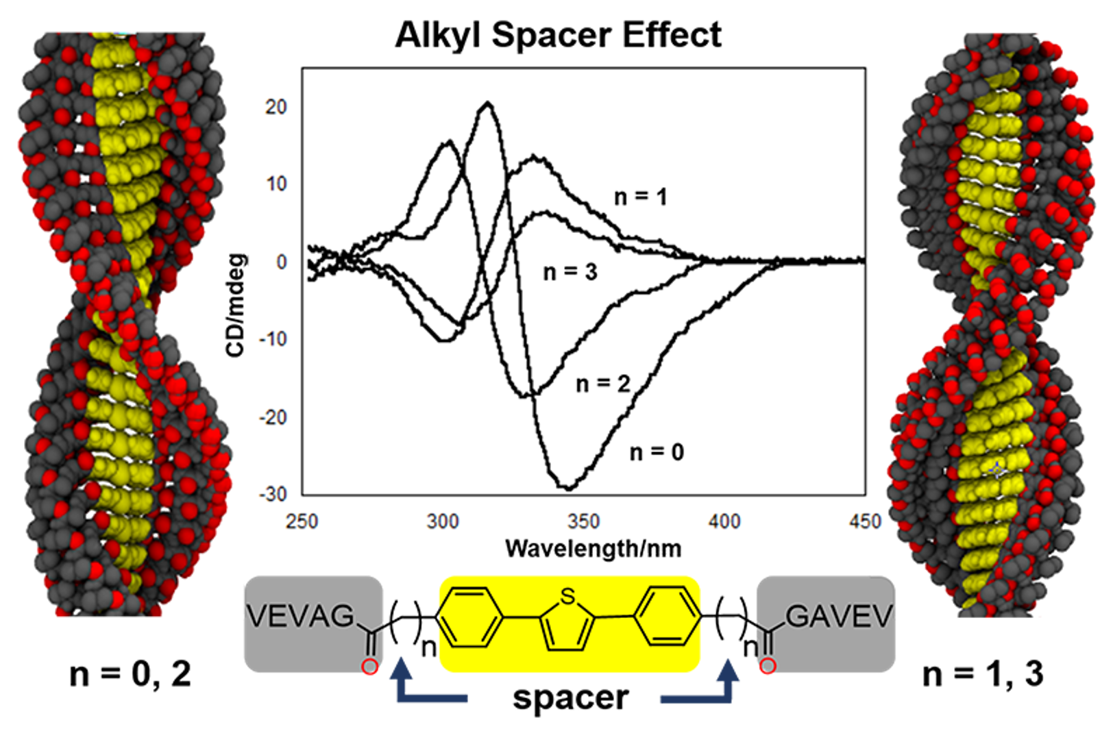
Synthetic peptide libraries to probe chiroptical properties.We found that carbon spacers between pi-conjugated electronic units and flanking peptide sequences had a profound impact on the superstructural chirality of the nanomaterials that form after self-assembly. The origins of this control were elucidated through computational analysis. These findings are of importance for chiroptical applications such as circularly polarized luminescence.
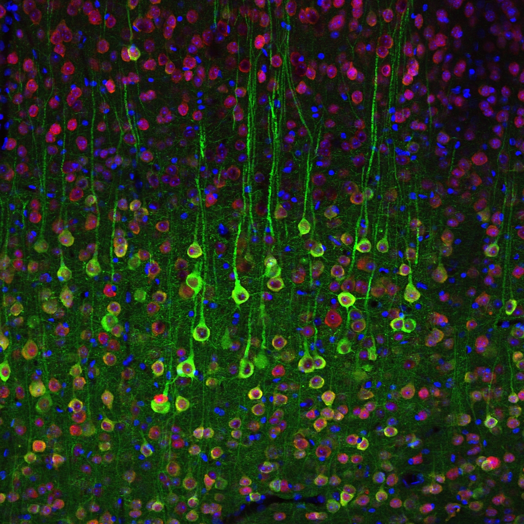
Self-assembled Peptide-p-electron Supramolecular Polymers for Bioinspired Energy Harvesting, Transport and Management
2/8/2023 | J. Tovar, H. Katz (Johns Hopkins U.) and A. Ferguson (U. Chicago)
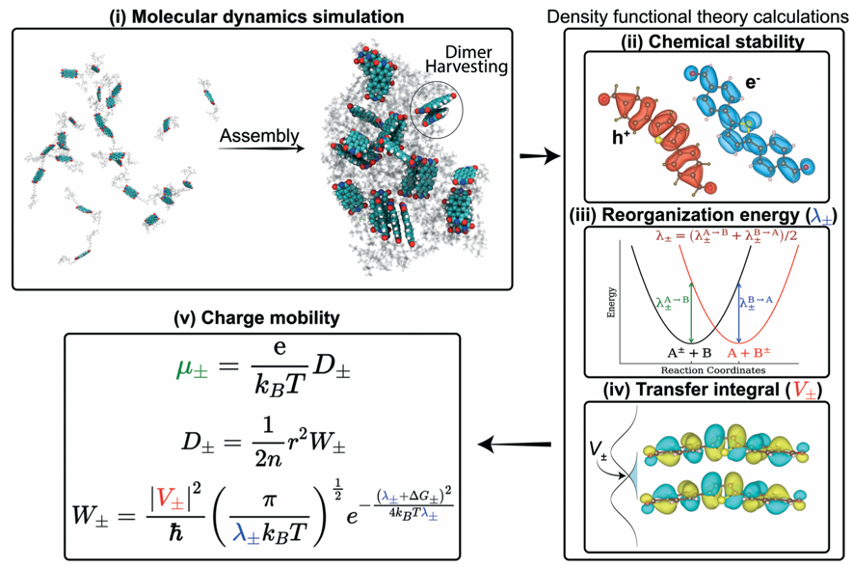
Organic electronics offer a route toward electronically active biocompatible soft materials capable of interfacing with biological and living systems. Discovering new organic molecules capable of high charge mobility is challenging due to the vast size of molecular design space and the multi-scale nature of charge transport that requires modeling electrons, molecules, and supramolecular assemblies.

Self-assembled Peptide-p-electron Supramolecular Polymers
2/8/2023 | A. Ferguson (U. Chicago)
Non-natural peptides containing electron-rich aromatic subunits have demonstrated the remarkable ability to spontaneously assemble into long fibers with optical and electronic responses similar to conventional silicon electronics. These molecules have the potential to serve as new biocompatible organic electronics with uses in medical interventions and clean energy.
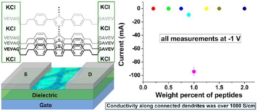
Conductive Organic-inorganic Nanostructures
2/8/2023 | J. Tovar and H. Katz (Johns Hopkins U.)
Dendritic structures assembled via connections between mineralizing KCl crystallites initiated by pH-triggered self-assembly of peptide materials was demonstrated. Connected structures were found to be the most important factor for producing highly conductive nanowire assemblies that showed conductivity comparable to that of a metal (~1800 S/cm). Measurements of conductivity over time and conductivity quenching by ammonia suggested the conductivity of these dendritic networks was derived from proton doping of the central π-electron units in strong acid environment and was facilitated by closely spaced chromophores leading to facile π-electron transfer along the interconnected dendritic pathways. It is expected that more electrically relevant materials may be able to be templated through this approach.
Self-assembled Peptide-p-electron Supramolecular Polymers for Bioinspired Energy Harvesting, Transport, and Management
2/8/2023 | J. Tovar (Johns Hopkins U.) and A. Ferguson (U. Chicago)
This project integrates experiment, simulation, and data-science to engineer supramolecular optoelectronic peptidic semiconductors.
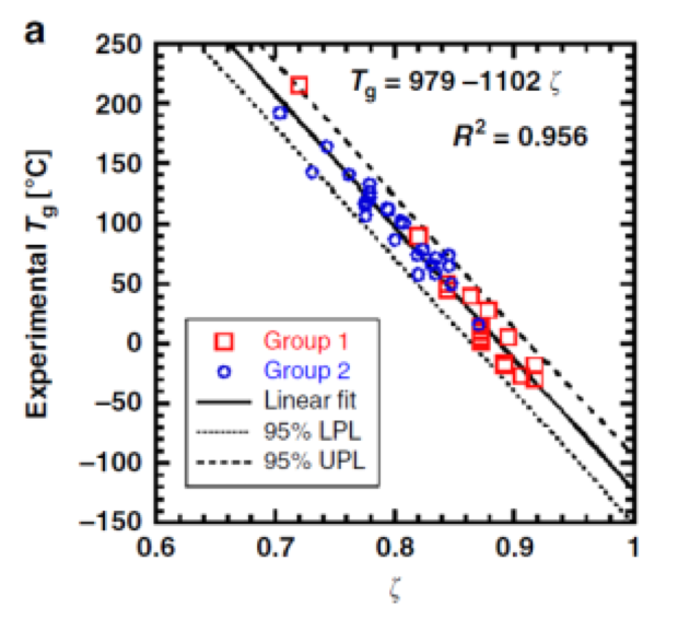
Glass Transition Temperature from the Chemical Structure of Conjugated Polymers
2/7/2023
The Tg demarks the transition into a brittle glassy state, making its accurate prediction for conjugated polymers crucial for the design of soft, stretchable, or flexible electronics.
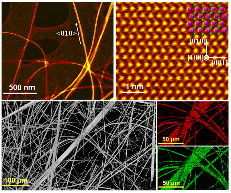
Unique Properties of One-Dimensional Materials
2/6/2023 | F. Homrich da Jornada (Stanford), A. A. Balandin, L. Bartels (U. CA – Riverside)
We synthesized and investigated MoI3, a van der Waals material with a “true one-dimensional” crystal structure that can be exfoliated to individual atomic chains. Machine learning allowed to establish the existence of MoI3 with 1D crystal structure as opposed to the previously suggested 2D structure.

Self-assembled peptide-pi-electron supramolecular polymers for bioinspired energy harvesting, transport and management
2/6/2023 | Andrew Ferguson, University of Chicago
Organic electronics offer a route toward electronically active biocompatible soft materials capable of interfacing with biological and living systems. Discovering new organic molecules capable of high charge mobility is challenging due to the vast size of molecular design space and the multi-scale nature of charge transport that requires modeling electrons, molecules, and supramolecular assemblies.
Showing 151 to 160 of 242