Research Highlights
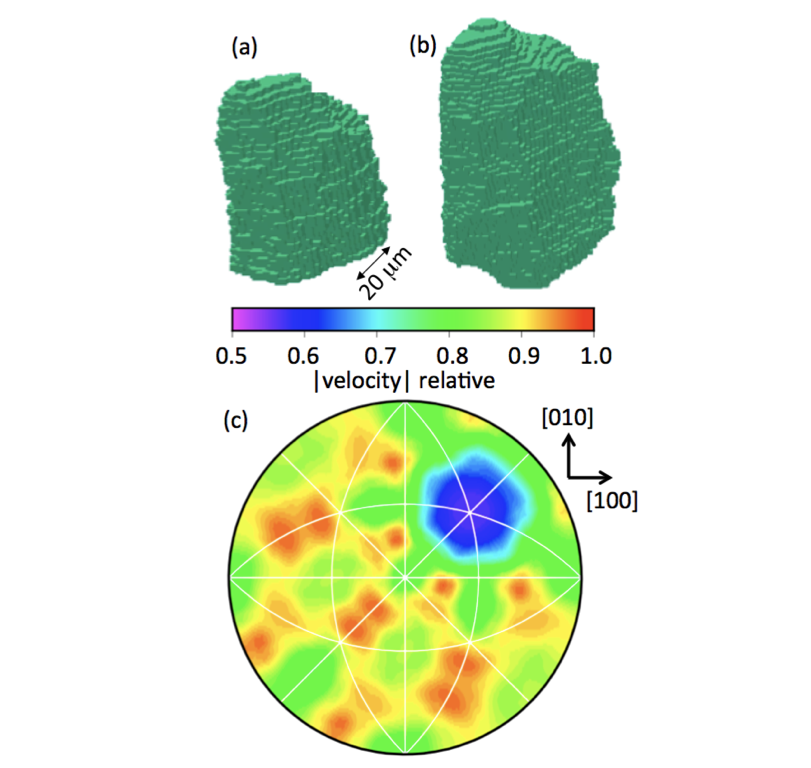
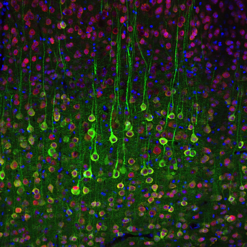
Grain Boundary Velocity Distributions
4/1/2019 | Gregory Rohrer, Robert Suter
Polycrystalline metals and ceramics are opaque to most forms of radiation. Because of this, it has not been possible to observe the motion of grain boundaries within a polycrystalline network.
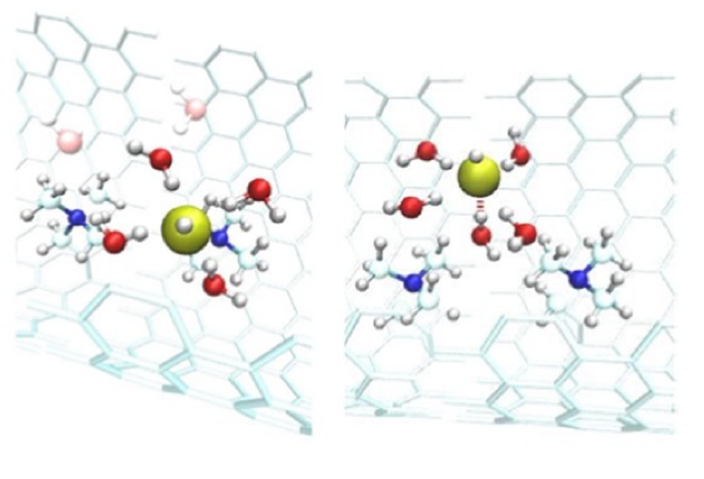
Hydroxide Diffusion in Anion Exchange Membranes
2/28/2019
The development of reliable, cost-effective polymer architectures for use as anion exchange membranes (AEMs) is an important challenge facing emerging electrochemical device technologies.
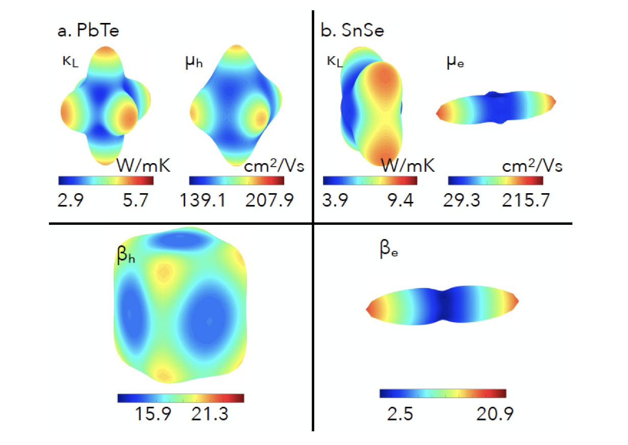
Predicting Anisotropic Performance in Thermoelectrics
2/15/2019 | Eric Toberer, Vladan Stevanovic
Anisotropic properties yield anisotropic thermoelectric performance. Heat maps show lattice thermal conductivity (kL), mobility (uH) and ultimate thermoelectric performance (b)

Double Doping of Organic Semiconducting Polymers
1/14/2019 | Seth Marder (Georgia Tech.)
Molecular doping is a crucial tool for controlling the number of charge carriers in organic semiconductors, which in turn tunes the conductivity of the materials.
Closed-loop Design of Heterostructures for Solar Energy Conversion
12/13/2018 | S. Banerjee (TAMU), D. Watson (U. Buffalo), and L. Piper (Binghamton)
Schematic illustration of CdSe/β-SnxV2O5 heterostructures that enable photocatalytic water splitting; Right: illustration of design of MxV2O5 compounds with p-block cations that yield mid-gap states.
A Simple and Robust Approach to Reducing Contact Resistance in Organic Transistors
12/1/2018 | Z. A. Lamport, K. J. Barth, H. Lee, E. Gann, S. Engmann, H. Chen, M. Guthold, I. McCulloch, J. E. Anthony, L. J. Richter, D. M. DeLongchamp, and O. D. Jurchescu
Contact effects limit device performance, even in the case of high-mobility semiconductors. We developed a strategy for drastically reducing contact effects: it consists in creating high work function domains at the surface of the injecting electrodes to promote channels of enhanced injection.
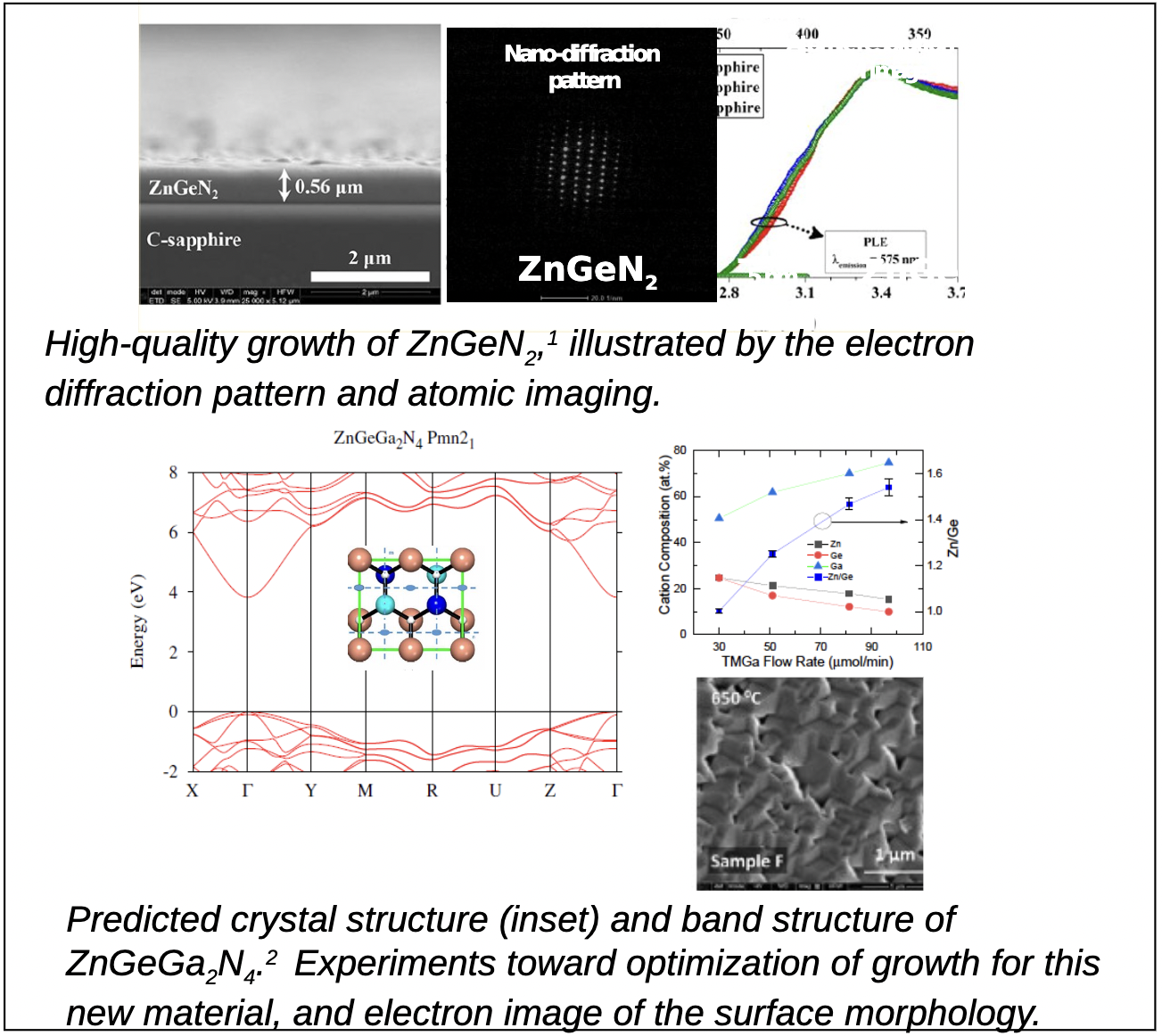
MOVCD of Complex Nitride Semiconductors
11/26/2018 | K. Kash, W. Lambrecht, H. Zhao
A unique, custom-designed research instrument for metal-organic chemical vapor deposition (MOCVD) is enabling the synthesis and study of complex nitride semiconductors, such as ZnGeN21, and alloys and heterostructures of these materials, alone and in combination with the binary nitrides (Al,Ga,In)
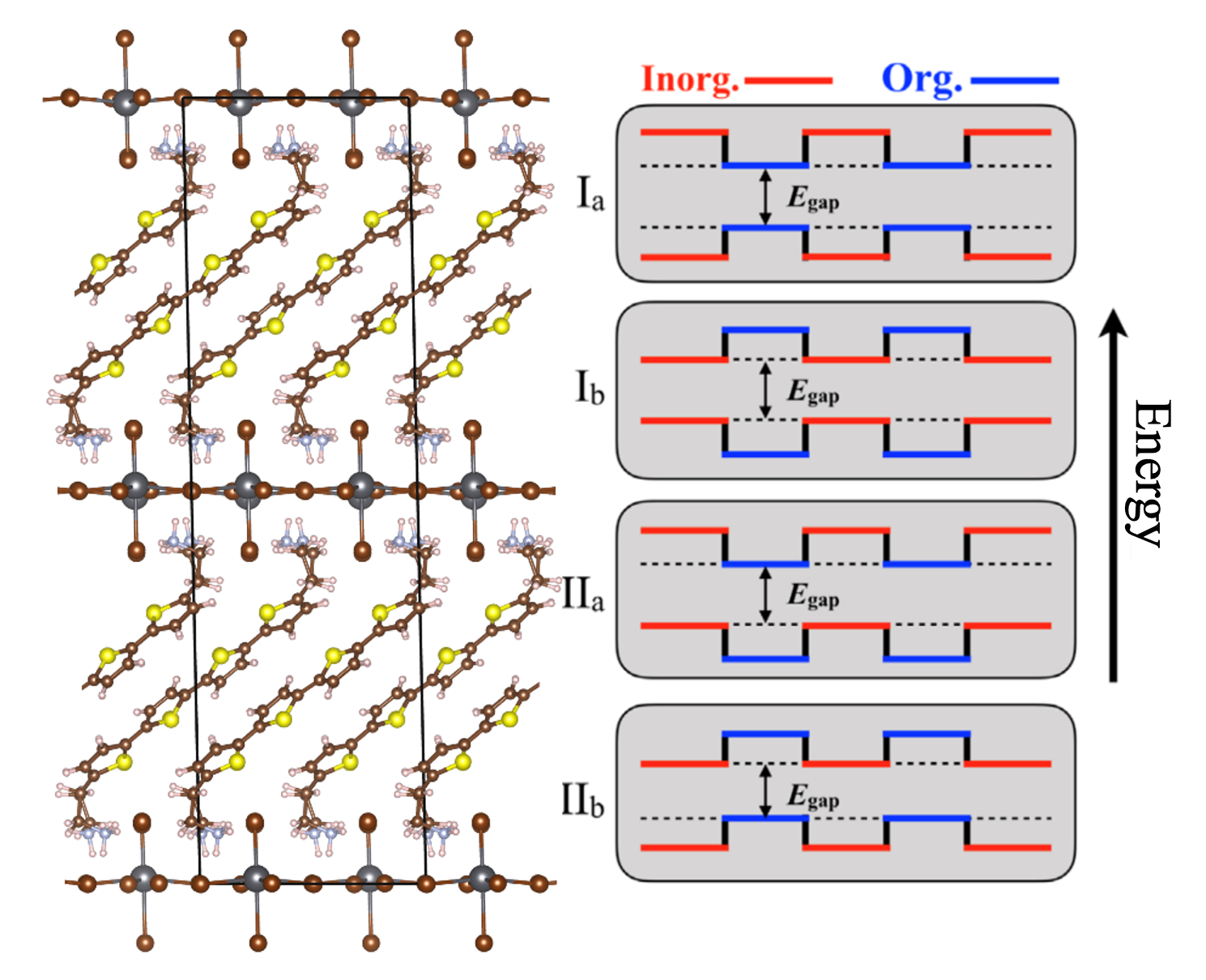
Tunable Semiconductors: Organic-inorganic Hybrids
10/4/2018 | W. You, Y. Kanai (U. NC); D. Mitzi, V. Blum (Duke U.)
We use high-level computational theory to demonstrate how a novel class of crystalline semiconductor materials, so-called layered hybrid organic-inorganic perovskites (HOIPs), can be designed at the atomic scale to provide targeted semiconductor properties. The tun-ability of the materials arises from the atomic-scale combination of an inorganic semi-conductor integrated with functionalized organic molecules that offer a wide range of properties.
Materials from Mathematics
8/30/2018 | Richard D. James, University of Minnesota
Austenite/martensite interface in Cu69.5Al27Ni3.5. Zero elastic energy austenite/martensite interfaces possible under the co-factor conditions. Red is austenite and blue/green are two variants of martensite. These pictures exhibit large deformations, zero elastic energy, and perfect fitting of the phases under continuous variation of the volume fraction f.
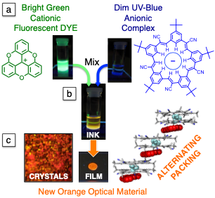
Controlling Emission in Optical Materials
8/21/2018 | Amar H. Flood (PI), Steven L. Tait, Krishnan Raghavachari, Peter J. Ortoleva
If we can understand how the packing gives rise to the optical properties, then we can control the packing to generate materials of any color and brightness.
Showing 211 to 220 of 242